ชาว ศวกรรมคอมพ วเตอร คณะว ศวกรรมศาสตร มหาว ทยาล ยเทคโนโลย ราชมงคลพระนคร
|
|
|
- Randolph Walker
- 5 years ago
- Views:
Transcription


1 EN วงจรไฟฟ าและอ เล กทรอน กส Circuits and Electronics บทท 7 ทรานซ สเตอร Bipolar Junction Transistor สาขาว ชาว ศวกรรมคอมพ วเตอร คณะว ศวกรรมศาสตร มหาว ทยาล ยเทคโนโลย ราชมงคลพระนคร
2 Objectives Describe the basic structure of the bipolar junction transistor (BJT) Explain and analyze basic transistor bias and operation Discuss the parameters and characteristics of a transistor and how they apply to transistor circuits Discuss how a transistor can be used as an amplifier or a switch Troubleshoot various failures typical of transistor circuits
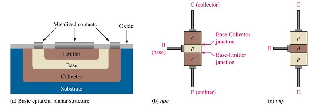
3 BJT Construction With diodes there is one p-n junction. With bipolar junction transistors (BJT), there are three three layers and two p-n junctions. Transistors can be a either pnp or npn type. The emitter (E) and is heavily doped (n-type). The collector (C) is also doped (n-type). The base (B) is lightly doped with opposite type to the emitter and collector (i.e. p-type in the npn transistor). The base is physically very thin. The p-n junction joining the base and emitter regions is called the baseemitter (B-E) junction. (or emitter-base, it doesn t really matter) The p-n junction between the base and collector regions is called the collector-base (C-B) junction.(or base-collector)
4 BJT Construction

5 Symbols

6 Current Flows The forward bias between the base and emitter injects electrons from the emitter into the base and holes from the base into the emitter. As the emitter is heavily doped and the base lightly doped most of the current transport across this junction is due to the electrons flowing from emitter to base The base is lightly doped and physically very thin. Thus only a small percentage of electrons flowing across the base-emitter (BE) junction combine with the available holes in this region. I E = I C + I B
7 BJT Operation A transistor is a device which can be used as either an: Amplifier Switch Let s first consider it s operation in a more simple view as a current controlling device.
8 BJT Operation Look at this one circuit as two separate circuits: base-emitter(left side) circuit collector-emitter(right side) circuit. Note that the emitter leg serves as a conductor for both circuits. The amount of current flow in the base-emitter circuit controls the amount of current that flows in the collector circuit. Small changes in base-emitter current yields a large change in collector-current. I C is approx 100 times I B (ratio is called beta )
9 Modes of Operation Depending on the bias condition (forward or reverse) of each of the two junctions, there are different modes of operation of the BJT. Modes EBJ CBJ Application Cutoff Reverse Reverse Saturation Forward Forward Switching application in digital circuits Active Forward Reverse Amplifier Reverse active Reverse Forward Performance degradation

10 Amplification
11 Input Characteristics The ic-vbe characteristic for an npn transistor
12 Output Characteristics I C (ma) Saturation Region Active Region I B = 200 ma I B = 150 ma 15 I B = 100 ma Cutoff Region I B = 50 ma I B = 0 V CE (V)
13 Transistor Characteristics and Parameters As previously discussed, base-emitter current changes yields large changes in collector-emitter current. The factor of this change is called beta( ). DC = I C /I B α DC = I C / I E
14 Transistor Characteristics and Parameters There are three key dc voltages and three key dc currents to be considered. Note that these measurements are important for troubleshooting.
15 Transistor Characteristics and Parameters I B : dc base current I E : dc emitter current I C : dc collector current V BE : dc voltage across base-emitter junction V CB : dc voltage across collector-base junction V CE : dc voltage from collector to emitter
16 Transistors Characteristics and Parameters For proper operation the base-emitter junction is forward biased by V BB and conducts just like a diode. The collector-base junction is reverse biased by V CC and blocks current flow through it s junction just like a diode.
17 Transistors Characteristics and Parameters Remember current flow through the base-emitter junction will help establish the path for current flow from the collector to emitter.
18 Transistor Characteristics and Parameters Analysis of this transistor circuit to predict the dc voltages and currents requires use of Ohm s law, Kirchhoff s voltage law and the beta for the transistor. Application of these laws begins with the base circuit to determine the amount of base current. Using Kirchhoff's voltage law, subtract the 0.7 V BE and the remaining voltage is dropped across R B. Determining the current for the base with this information is a matter of applying of Ohm s law. I B = ( V BB V BE )/R B
19 Transistor Characteristics and Parameters I C = I B I E = I C + I B V BE = 0.7 (Will be used in most analysis examples) V CE = V CC V RC = V CC I C R C V CB = V CE - V BE
20 Transistor Characteristics and Parameters What we ultimately determine by use of Kirchhoff s voltage law for series circuits is that in the base circuit V BB is distributed across the base-emitter junction and R B in the base circuit. In the collector circuit we determine that V CC is distributed proportionally across R C and the transistor(v CE ).
21 Example Find out the DC Currents and Voltages in the CCT.
22 Transistor Characteristics and Parameters Collector characteristic curves gives a graphical illustration of the relationship of collector current and V CE with specified amounts of base current. With greater increases of V CC, V CE continues to increase until it reaches breakdown, but the current remains about the same in the linear region from.7v to the breakdown voltage.
23 Transistor Characteristics and Parameters With no I B the transistor is in the cutoff region and just as the name implies there is practically no current flow in the collector part of the circuit. With the transistor in a cutoff state the the full V CC can be measured across the collector and emitter(v CE )
24 Transistor Characteristics and Parameters Current flow in the collector part of the circuit is, as stated previously, determined by I B multiplied by. However, there is a limit to how much current can flow in the collector circuit regardless of additional increases in I B.
25 Transistor Characteristics and Parameters Once this maximum is reached, the transistor is said to be in saturation. Note that saturation can be determined by application of Ohm s law. I C(sat) =V CC /R C The measured voltage across this now seemingly shorted collector and emitter is 0V.
26 Transistor Characteristics and Parameters The dc load line graphically illustrates I C(sat) and Cutoff for a transistor.
27 Example Determine whether or not the transistor is in saturation region. Assume V CE(sat) =0.2V. Steps: 1. Find I C(sat) 2. Find I B 3. Find I C for I B 4. If I C > I C(sat) The BJT is in saturation region. Can I C ever exceed I C(sat) in normal operation????


28 Transistor Characteristics and Parameters The beta for a transistor is not always constant. Temperature and collector current both affect beta, not to mention the normal inconsistencies during the manufacture of the transistor. There are also maximum power ratings to consider. The data sheet provides information on these characteristics.
29 Example P D(max) =800mW, V CE(max) =15V, I C(max) =100mA Determine the maximum value of V CC that can be adjusted without exceeding a rating. Which rating will be crossed first? Steps: 1. Determine I B 2. Determine I C for I B 3. I C > I C(max)??? 4. What will be the max value of V CC for which V CE = 15V for calculated value of I C?? 5. Calculate P D 6. P D > P D(max)??? 7. What if V BB is cut out???
30 Transistor Amplifier Amplification of a relatively small ac voltage can be had by placing the ac signal source in the base circuit. Recall that small changes in the base current circuit causes large changes in collector current circuit. The small ac voltage causes the base current to increase and decrease accordingly and with this small change in current the collector current will mimic the input only with greater amplitude.
31 Transistor Amplifier I e = V b / r e = I c V c = I c R C A v = V out / V in = V c / V b = I c R C / I e r e A v = R C / r e
32 Transistor Switch A transistor when used as a switch is simply being biased so that it is in cutoff (switched off) or saturation (switched on). Remember that the V CE in cutoff is V CC and 0V in saturation. Cut off: I B = 0 I C = 0 V CE = V CC Saturation: I C =(V CC V CE(sat) )/R C I B(min) = I C(sat) / β DC V CE = 0 ideally or few tens of a volt. Some text assume V CE(sat) = 0.2V
33 Troubleshooting Troubleshooting a live transistor circuit requires us to be familiar with known good voltages, but some general rules do apply. Certainly a solid fundamental understanding of Ohm s law and Kirchhoff s voltage and current laws is imperative. With live circuits it is most practical to troubleshoot with voltage measurements.
34 Troubleshooting Opens in the external resistors or connections of the base or the circuit collector circuit would cause current to cease in the collector and the voltage measurements would indicate this. Internal opens within the transistor itself could also cause transistor operation to cease. Erroneous voltage measurements that are typically low are a result of point that is not solidly connected. This called a floating point. This is typically indicative of an open. More in-depth discussion of typical failures are discussed within the textbook.

35 Troubleshooting Testing a transistor can be viewed more simply if you view it as testing two diode junctions. Forward bias having low resistance and reverse bias having infinite resistance.

36 Troubleshooting The diode test function of a multimeter is more reliable than using an ohmmeter. Make sure to note whether it is an npn or pnp and polarize the test leads accordingly.
37 Troubleshooting In addition to the traditional DMMs there are also transistor testers. Some of these have the ability to test other parameters of the transistor, such as leakage and gain. Curve tracers give us even more detailed information about a transistors characteristics.
38 Summary The bipolarjunction transistor (BJT) is constructed of three regions: base, collector, and emitter. The BJT has two pn junctions, the base-emitter junction and the basecollector junction. The two types of transistors are pnp and npn. For the BJT to operate as an amplifier, the base-emitter junction is forward biased and the collector-base junction is reverse biased. Of the three currents I B is very small in comparison to I E and I C. Beta is the current gain of a transistor. This the ratio of I C /I B.
39 Summary A transistor can be operated as an electronics switch. When the transistor is off it is in cutoff condition (no current). When the transistor is on, it is in saturation condition (maximum current). Beta can vary with temperature and also varies from transistor to transistor.
 = 0V 3.")
40 Quiz 1. If V IN = 0, V CE =?? 2. I B(min) =?? for saturating transistor. β DC = 200, V CE(sat) = 0V 3. R B(max) when V IN = 5V
41
Bipolar Junction Transistor (BJT)
") Bipolar Junction Transistor (BJT) 1 Objectives To understand the structure of BJT. To explain and analyze the basic transistor circuits. To use transistors as an amplifier and electronic switch. To design
Bipolar Junction Transistor (BJT) 1 Objectives To understand the structure of BJT. To explain and analyze the basic transistor circuits. To use transistors as an amplifier and electronic switch. To design
ชาว ศวกรรมคอมพ วเตอร คณะว ศวกรรมศาสตร มหาว ทยาล ยเทคโนโลย ราชมงคลพระนคร
 EN2042102 วงจรไฟฟ าและอ เล กทรอน กส Circuits and Electronics บทท 5 สารก งต วน า Semiconductor สาขาว ชาว ศวกรรมคอมพ วเตอร คณะว ศวกรรมศาสตร มหาว ทยาล ยเทคโนโลย ราชมงคลพระนคร Bohr model of an atom As seen
ITT Technical Institute. ET215 Devices 1. Unit 6 Chapter 3, Sections
 ITT Technical Institute ET215 Devices 1 Unit 6 Chapter 3, Sections 3.7-3.9 Chapter 3 Section 3.7 The Bipolar Transistor as a Switch Objectives: Explain how a transistor can be used as a switch 1. Compute
Lecture 24: Bipolar Junction Transistors (1) Bipolar Junction Structure, Operating Regions, Biasing
 Bipolar Junction Structure, Operating Regions, Biasing") Lecture 24: Bipolar Junction Transistors (1) Bipolar Junction Structure, Operating Regions, Biasing BJT Structure the BJT is formed by doping three semiconductor regions (emitter, base, and collector)
Lecture 24: Bipolar Junction Transistors (1) Bipolar Junction Structure, Operating Regions, Biasing BJT Structure the BJT is formed by doping three semiconductor regions (emitter, base, and collector)
ET215 Devices I Unit 4A
 ITT Technical Institute ET215 Devices I Unit 4A Chapter 3, Section 3.1-3.2 This unit is divided into two parts; Unit 4A and Unit 4B Chapter 3 Section 3.1 Structure of Bipolar Junction Transistors The basic
EXPERIMENT 5 CURRENT AND VOLTAGE CHARACTERISTICS OF BJT
 EXPERIMENT 5 CURRENT AND VOLTAGE CHARACTERISTICS OF BJT 1. OBJECTIVES 1.1 To practice how to test NPN and PNP transistors using multimeter. 1.2 To demonstrate the relationship between collector current
Analog Electronics. Electronic Devices, 9th edition Thomas L. Floyd Pearson Education. Upper Saddle River, NJ, All rights reserved.
 Analog Electronics BJT Structure The BJT has three regions called the emitter, base, and collector. Between the regions are junctions as indicated. The base is a thin lightly doped region compared to the
Electronics II Lecture 2(a): Bipolar Junction Transistors
: Bipolar Junction Transistors") Lecture 2(a): Bipolar Junction Transistors A/Lectr. Khalid Shakir Dept. Of Engineering Engineering by Pearson Transistor! Transistor=Transfer+Resistor. When Transistor operates in active region its input
Lecture 2(a): Bipolar Junction Transistors A/Lectr. Khalid Shakir Dept. Of Engineering Engineering by Pearson Transistor! Transistor=Transfer+Resistor. When Transistor operates in active region its input
Chapter 3: Bipolar Junction Transistors
 Chapter 3: Bipolar Junction Transistors Transistor Construction There are two types of transistors: pnp npn pnp The terminals are labeled: E - Emitter B - Base C - Collector npn 2 Transistor Operation
Lecture 12. Bipolar Junction Transistor (BJT) BJT 1-1
 BJT 1-1") Lecture 12 Bipolar Junction Transistor (BJT) BJT 1-1 Course Info Lecture hours: 4 Two Lectures weekly (Saturdays and Wednesdays) Location: K2 Time: 1:40 pm Tutorial hours: 2 One tutorial class every week
Lecture 12 Bipolar Junction Transistor (BJT) BJT 1-1 Course Info Lecture hours: 4 Two Lectures weekly (Saturdays and Wednesdays) Location: K2 Time: 1:40 pm Tutorial hours: 2 One tutorial class every week
EN วงจรไฟฟ าและอ เล กทรอน กส Circuits and Electronics บทท 2 พ นฐานวงจรไฟฟ า
 EN2042102 วงจรไฟฟ าและอ เล กทรอน กส Circuits and Electronics บทท 2 พ นฐานวงจรไฟฟ า สาขาว ชาว ศวกรรมคอมพ วเตอร คณะว ศวกรรมศาสตร มหาว ทยาล ยเทคโนโลย ราชมงคลพระนคร INTRODUCTION Two types of current are readily
Chapter 3 Bipolar Junction Transistors (BJT)
") Chapter 3 Bipolar Junction Transistors (BJT) Transistors In analog circuits, transistors are used in amplifiers and linear regulated power supplies. In digital circuits they function as electrical switches,
Chapter 3 Bipolar Junction Transistors (BJT) Transistors In analog circuits, transistors are used in amplifiers and linear regulated power supplies. In digital circuits they function as electrical switches,
Bipolar Junction Transistors
 Bipolar Junction Transistors Invented in 1948 at Bell Telephone laboratories Bipolar junction transistor (BJT) - one of the major three terminal devices Three terminal devices more useful than two terminal
COE/EE152: Basic Electronics. Lecture 5. Andrew Selasi Agbemenu. Outline
 COE/EE152: Basic Electronics Lecture 5 Andrew Selasi Agbemenu 1 Outline Physical Structure of BJT Two Diode Analogy Modes of Operation Forward Active Mode of BJTs BJT Configurations Early Effect Large
Figure1: Basic BJT construction.
 Chapter 4: Bipolar Junction Transistors (BJTs) Bipolar Junction Transistor (BJT) Structure The BJT is constructed with three doped semiconductor regions separated by two pn junctions, as in Figure 1(a).
Bipolar Junction Transistors (BJTs)
") C H A P T E R 6 Bipolar Junction Transistors (BJTs) Figure 6.1 A simplified structure of the npn transistor and pnp transistor. Table 6.1: BJT modes of Operation Mode Cutoff Active Saturation EBJ Reverse
C H A P T E R 6 Bipolar Junction Transistors (BJTs) Figure 6.1 A simplified structure of the npn transistor and pnp transistor. Table 6.1: BJT modes of Operation Mode Cutoff Active Saturation EBJ Reverse
Bipolar Junction Transistors (BJTs) Overview
 Overview") 1 Bipolar Junction Transistors (BJTs) Asst. Prof. MONTREE SIRIPRUCHYANUN, D. Eng. Dept. of Teacher Training in Electrical Engineering, Faculty of Technical Education King Mongkut s Institute of Technology
1 Bipolar Junction Transistors (BJTs) Asst. Prof. MONTREE SIRIPRUCHYANUN, D. Eng. Dept. of Teacher Training in Electrical Engineering, Faculty of Technical Education King Mongkut s Institute of Technology
BJT. Bipolar Junction Transistor BJT BJT 11/6/2018. Dr. Satish Chandra, Assistant Professor, P P N College, Kanpur 1
 BJT Bipolar Junction Transistor Satish Chandra Assistant Professor Department of Physics P P N College, Kanpur www.satish0402.weebly.com The Bipolar Junction Transistor is a semiconductor device which
Lecture 3: Transistors
 Lecture 3: Transistors Now that we know about diodes, let s put two of them together, as follows: collector base emitter n p n moderately doped lightly doped, and very thin heavily doped At first glance,
ELEC 2210 EXPERIMENT 7 The Bipolar Junction Transistor (BJT)
") ELEC 2210 EXPERIMENT 7 The Bipolar Junction Transistor (BJT) Objectives: The experiments in this laboratory exercise will provide an introduction to the BJT. You will use the Bit Bucket breadboarding system
ELEC 2210 EXPERIMENT 7 The Bipolar Junction Transistor (BJT) Objectives: The experiments in this laboratory exercise will provide an introduction to the BJT. You will use the Bit Bucket breadboarding system
5.1 BJT Device Structure and Physical Operation
 11/28/2004 section 5_1 BJT Device Structure and Physical Operation blank 1/2 5.1 BJT Device Structure and Physical Operation Reading Assignment: pp. 377-392 Another kind of transistor is the Bipolar Junction
Lecture (06) Bipolar Junction Transistor
 Bipolar Junction Transistor") Lecture (06) Bipolar Junction Transistor By: Dr. Ahmed lshafee ١ Agenda BJT structure BJT operation BJT characteristics ٢ BJT structure The BJT is constructed with three doped semiconductor regions One
Lecture (06) Bipolar Junction Transistor By: Dr. Ahmed lshafee ١ Agenda BJT structure BJT operation BJT characteristics ٢ BJT structure The BJT is constructed with three doped semiconductor regions One
C H A P T E R 6 Bipolar Junction Transistors (BJTs)
") C H A P T E R 6 Bipolar Junction Transistors (BJTs) Figure 6.1 A simplified structure of the npn transistor and pnp transistor. Table 6.1: BJT modes of Operation Mode EBJ CBJ Cutoff Reverse Reverse Active
C H A P T E R 6 Bipolar Junction Transistors (BJTs) Figure 6.1 A simplified structure of the npn transistor and pnp transistor. Table 6.1: BJT modes of Operation Mode EBJ CBJ Cutoff Reverse Reverse Active
Chapter 4 DC Biasing BJTs. BJTs
 hapter 4 D Biasing BJTs BJTs Biasing Biasing: The D voltages applied to a transistor in order to turn it on so that it can amplify the A signal. Operating Point The D input establishes an operating or
Physics of Bipolar Transistor
 Physics of Bipolar Transistor Motivations - In many electronic applications, amplifier is the most fundamental building block. Ex Audio amplifier: amplifies electric signal to drive a speaker RF Power
Tutorial 2 BJTs, Transistor Bias Circuits, BJT Amplifiers FETs and FETs Amplifiers. Part 1: BJTs, Transistor Bias Circuits and BJT Amplifiers
 Tutorial 2 BJTs, Transistor Bias Circuits, BJT Amplifiers FETs and FETs Amplifiers Part 1: BJTs, Transistor Bias Circuits and BJT Amplifiers 1. Explain the purpose of a thin, lightly doped base region.
Analog & Digital Electronics Course No: PH-218
 Analog & Digital Electronics Course No: PH-218 Lec-5: Bipolar Junction Transistor (BJT) Course nstructors: Dr. A. P. VAJPEY Department of Physics, ndian nstitute of Technology Guwahati, ndia 1 Bipolar
Chapter 3. Bipolar Junction Transistors
 Chapter 3. Bipolar Junction Transistors Outline: Fundamental of Transistor Common-Base Configuration Common-Emitter Configuration Common-Collector Configuration Introduction The transistor is a three-layer
4.1.3 Structure of Actual Transistors
 4.1.3 Structure of Actual Transistors Figure 4.7 shows a more realistic BJT cross-section Collector virtually surrounds entire emitter region This makes it difficult for electrons injected into base to
Structure of Actual Transistors
 4.1.3. Structure of Actual Transistors Figure 4.7 shows a more realistic BJT cross-section Collector virtually surrounds entire emitter region This makes it difficult for electrons injected into base to
Chapter Two "Bipolar Transistor Circuits"
 Chapter Two "Bipolar Transistor Circuits" 1.TRANSISTOR CONSTRUCTION:- The transistor is a three-layer semiconductor device consisting of either two n- and one p-type layers of material or two p- and one
Chapter 3-2 Semiconductor devices Transistors and Amplifiers-BJT Department of Mechanical Engineering
 MEMS1082 Chapter 3-2 Semiconductor devices Transistors and Amplifiers-BJT Bipolar Transistor Construction npn BJT Transistor Structure npn BJT I = I + E C I B V V BE CE = V = V B C V V E E Base-to-emitter
Communication Microelectronics (W17)
") Communication Microelectronics (W17) Lecture 4: Bipolar Junction Transistor Assistant Professor Office: C3.315 E-mail: eman.azab@guc.edu.eg 1 Bipolar Junction Transistor (BJT) Physical Structure and I-V
Communication Microelectronics (W17) Lecture 4: Bipolar Junction Transistor Assistant Professor Office: C3.315 E-mail: eman.azab@guc.edu.eg 1 Bipolar Junction Transistor (BJT) Physical Structure and I-V
EE105 Fall 2014 Microelectronic Devices and Circuits. NPN Bipolar Junction Transistor (BJT)
") EE105 Fall 2014 Microelectronic Devices and Circuits Prof. Ming C. Wu wu@eecs.berkeley.edu 511 utardja Dai Hall (DH) 1 NPN Bipolar Junction Transistor (BJT) Forward Bias Reverse Bias Hole Flow Electron
EE105 Fall 2014 Microelectronic Devices and Circuits Prof. Ming C. Wu wu@eecs.berkeley.edu 511 utardja Dai Hall (DH) 1 NPN Bipolar Junction Transistor (BJT) Forward Bias Reverse Bias Hole Flow Electron
KOM2751 Analog Electronics :: Dr. Muharrem Mercimek :: YTU - Control and Automation Dept. 1 2 (CONT D - II) DIODE APPLICATIONS
 DIODE APPLICATIONS") KOM2751 Analog Electronics :: Dr. Muharrem Mercimek :: YTU - Control and Automation Dept. 1 2 (CONT D - II) DIODE APPLICATIONS Most of the content is from the textbook: Electronic devices and circuit theory,
KOM2751 Analog Electronics :: Dr. Muharrem Mercimek :: YTU - Control and Automation Dept. 1 2 (CONT D - II) DIODE APPLICATIONS Most of the content is from the textbook: Electronic devices and circuit theory,
การไบอ สทรานซ สเตอร. Transistors Biasing
 การไบอ สทรานซ สเตอร Transistors iasing iasing iasing: Applying D voltages to a transistor in order to turn it on so that it can amplify A signals. The D input establishes an operating or quiescent point
CHAPTER 3: BIPOLAR JUNCION TRANSISTOR DR. PHẠM NGUYỄN THANH LOAN
 CHAPTER 3: BIPOLAR JUNCION TRANSISTOR DR. PHẠM NGUYỄN THANH LOAN Hanoi, 9/24/2012 Contents 2 Structure and operation of BJT Different configurations of BJT Characteristic curves DC biasing method and analysis
EET1240/ET212 EET1240/ET212
 EET1240/ET212 Electronics Semiconductors and Diodes Electrical and Telecommunications Engineering Technology Department Prepared by textbook based on Electronics Devices by Floyd, Prentice Hall, 7 th edition.
ชาว ศวกรรมคอมพ วเตอร คณะว ศวกรรมศาสตร มหาว ทยาล ยเทคโนโลย ราชมงคลพระนคร
 EN2042102 วงจรไฟฟ าและอ เล กทรอน กส Circuits and Electronics บทท 6 ไดโอด Diode สาขาว ชาว ศวกรรมคอมพ วเตอร คณะว ศวกรรมศาสตร มหาว ทยาล ยเทคโนโลย ราชมงคลพระนคร Objectives Explain and analyze the operation
ECE321 Electronics I Fall 2006
 ECE321 Electronics I Fall 2006 Professor James E. Morris Lecture 11 31 st October, 2006 Bipolar Junction Transistors (BJTs) 5.1 Device Structure & Physics 5.2 I-V Characteristics Convert 5.1 information
The shape of the waveform will be the same, but its level is shifted either upward or downward. The values of the resistor R and capacitor C affect
 Diode as Clamper A clamping circuit is used to place either the positive or negative peak of a signal at a desired level. The dc component is simply added or subtracted to/from the input signal. The clamper
Transistors and Applications
 Chapter 17 Transistors and Applications DC Operation of Bipolar Junction Transistors (BJTs) The bipolar junction transistor (BJT) is constructed with three doped semiconductor regions separated by two
Exercises 6.1, 6.2, 6.3 (page 315 on 7 th edition textbook)
") Exercises 6.1, 6.2, 6.3 (page 315 on 7 th edition textbook) Recapitulation and Equivalent Circuit Models Previous slides present first order BJT model. Assumes npn transistor in active mode. Basic relationship
Exercises 6.1, 6.2, 6.3 (page 315 on 7 th edition textbook) Recapitulation and Equivalent Circuit Models Previous slides present first order BJT model. Assumes npn transistor in active mode. Basic relationship
ECE 334: Electronic Circuits Lecture 2: BJT Large Signal Model
 Faculty of Engineering ECE 334: Electronic Circuits Lecture 2: BJT Large Signal Model Agenda I & V Notations BJT Devices & Symbols BJT Large Signal Model 2 I, V Notations (1) It is critical to understand
Electronics EECE2412 Spring 2017 Exam #2
 Electronics EECE2412 Spring 2017 Exam #2 Prof. Charles A. DiMarzio Department of Electrical and Computer Engineering Northeastern University 30 March 2017 File:12198/exams/exam2 Name: : General Rules:
14. Transistor Characteristics Lab
 1 14. Transistor Characteristics Lab Introduction Transistors are the active component in various devices like amplifiers and oscillators. They are called active devices since transistors are capable of
Basic Electronics Prof. Dr. Chitralekha Mahanta Department of Electronics and Communication Engineering Indian Institute of Technology, Guwahati
 Basic Electronics Prof. Dr. Chitralekha Mahanta Department of Electronics and Communication Engineering Indian Institute of Technology, Guwahati Module: 2 Bipolar Junction Transistors Lecture-1 Transistor
7. Bipolar Junction Transistor
 41 7. Bipolar Junction Transistor 7.1. Objectives - To experimentally examine the principles of operation of bipolar junction transistor (BJT); - To measure basic characteristics of n-p-n silicon transistor
Electronic Circuits - Tutorial 07 BJT transistor 1
 Electronic Circuits - Tutorial 07 BJT transistor 1-1 / 20 - T & F # Question 1 A bipolar junction transistor has three terminals. T 2 For operation in the linear or active region, the base-emitter junction
Module 2. B.Sc. I Electronics. Developed by: Mrs. Neha S. Joshi Asst. Professor Department of Electronics Willingdon College, Sangli
 Module 2 B.Sc. I Electronics Developed by: Mrs. Neha S. Joshi Asst. Professor Department of Electronics Willingdon College, Sangli BIPOLAR JUNCTION TRANSISTOR SCOPE OF THE CHAPTER- This chapter introduces
Transistor Characteristics
 Transistor Characteristics Topics covered in this presentation: Transistor Construction Transistor Operation Transistor Characteristics 1 of 15 The Transistor The transistor is a semiconductor device that
Exercise 2: Collector Current Versus Base Current
 Exercise 2: Collector Current Versus Base Current EXERCISE OBJECTIVE When you have completed this exercise, you will be able to demonstrate the relationship of collector current to base current by using
Microelectronic Circuits, Kyung Hee Univ. Spring, Bipolar Junction Transistors
 Bipolar Junction Transistors 1 Introduction physical structure of the bipolar transistor and how it works How the voltage between two terminals of the transistor controls the current that flows through
Chapter 5 Transistor Bias Circuits
 Chapter 5 Transistor Bias Circuits Objectives Discuss the concept of dc biasing of a transistor for linear operation Analyze voltage-divider bias, base bias, and collector-feedback bias circuits. Basic
Bipolar junction transistors.
 Bipolar junction transistors. Third Semester Course code : 15EECC202 Analog electronic circuits (AEC) Team: Dr. Nalini C Iyer, R.V. Hangal, Sujata N, Prashant A, Sneha Meti AEC Team, Faculty, School of
UNIT-III Bipolar Junction Transistor
 DC UNT-3.xplain the construction and working of JT. UNT- ipolar Junction Transistor A bipolar (junction) transistor (JT) is a three-terminal electronic device constructed of doped semiconductor material
Emitter base bias. Collector base bias Active Forward Reverse Saturation forward Forward Cut off Reverse Reverse Inverse Reverse Forward
 SEMICONDUCTOR PHYSICS-2 [Transistor, constructional characteristics, biasing of transistors, transistor configuration, transistor as an amplifier, transistor as a switch, transistor as an oscillator] Transistor
The collector terminal is common to the input and output signals and is connected to the dc power supply. Common Collector Circuit
 Common Collector Circuit When you have completed this exercise, you will be able to determine the dc operating conditions of a common collector (CC) transistor circuit by using a typical CC circuit. You
BFF1303: ELECTRICAL / ELECTRONICS ENGINEERING. Analog Electronics: Bipolar Junction Transistors
 BFF1303: ELECTRICAL / ELECTRONICS ENGINEERING Analog Electronics: Bipolar Junction Transistors Ismail Mohd Khairuddin, Zulkifil Md Yusof Faculty of Manufacturing Engineering Universiti Malaysia Pahang
ECE 440 Lecture 29 : Introduction to the BJT-I Class Outline:
 ECE 440 Lecture 29 : Introduction to the BJT-I Class Outline: Narrow-Base Diode BJT Fundamentals BJT Amplification Things you should know when you leave Key Questions How does the narrow-base diode multiply
DISCUSSION The best way to test a transistor is to connect it in a circuit that uses the transistor.
 Exercise 1: EXERCISE OBJECTIVE When you have completed this exercise, you will be able to test a transistor by forward biasing and reverse biasing the junctions. You will verify your results with an ohmmeter.
ECE 442 Solid State Devices & Circuits. 6. Bipolar Transistors
 ECE 442 Solid State Devices & Circuits 6. Bipolar Transistors Jose E. Schutt-Aine Electrical & Computer Engineering University of Illinois jschutt@emlab.uiuc.edu ECE 342 Jose Schutt Aine 1 Bipolar Junction
Transistor fundamentals Nafees Ahamad
 Transistor fundamentals Nafees Ahamad Asstt. Prof., EECE Deptt, DIT University, Dehradun Website: www.eedofdit.weebly.com Transistor A transistor consists of two PN junctions formed by sandwiching either
ECE 310 Microelectronics Circuits
 ECE 310 Microelectronics Circuits Bipolar Transistors Dr. Vishal Saxena (vishalsaxena@boisetstate.edu) Jan 20, 2014 Vishal Saxena 1 Bipolar Transistor n the chapter, we will study the physics of bipolar
UNIT 3 Transistors JFET
 UNIT 3 Transistors JFET Mosfet Definition of BJT A bipolar junction transistor is a three terminal semiconductor device consisting of two p-n junctions which is able to amplify or magnify a signal. It
An Introduction to Bipolar Junction Transistors. Prepared by Dr Yonas M Gebremichael, 2005
 An Introduction to Bipolar Junction Transistors Transistors Transistors are three port devices used in most integrated circuits such as amplifiers. Non amplifying components we have seen so far, such as
Analog Circuits Prof. Jayanta Mukherjee Department of Electrical Engineering Indian Institute of Technology - Bombay
 Analog Circuits Prof. Jayanta Mukherjee Department of Electrical Engineering Indian Institute of Technology - Bombay Week - 08 Module - 04 BJT DC Circuits Hello, welcome to another module of this course
Prof. Anyes Taffard. Physics 120/220. Diode Transistor
 Prof. Anyes Taffard Physics 120/220 Diode Transistor Diode One can think of a diode as a device which allows current to flow in only one direction. Anode I F Cathode stripe Diode conducts current in this
Lecture #3 BJT Transistors & DC Biasing
 November 2014 Ahmad El-Banna Integrated Technical Education Cluster At AlAmeeria J-601-1448 Electronic Principals Lecture #3 BJT Transistors & DC Biasing Instructor: Dr. Ahmad El-Banna Agenda Transistor
Electronic Devices. Floyd. Chapter 7. Ninth Edition. Electronic Devices, 9th edition Thomas L. Floyd
 Electronic Devices Ninth Edition Floyd Chapter 7 Power Amplifiers A power amplifier is a large signal amplifier that produces a replica of the input signal on its output. In the case shown here, the output
Current Mirrors. Basic BJT Current Mirror. Current mirrors are basic building blocks of analog design. Figure shows the basic NPN current mirror.
 Current Mirrors Basic BJT Current Mirror Current mirrors are basic building blocks of analog design. Figure shows the basic NPN current mirror. For its analysis, we assume identical transistors and neglect
Electronic Troubleshooting
 Electronic Troubleshooting Chapter 3 Bipolar Transistors Most devices still require some individual (discrete) transistors Used to customize operations Interface to external devices Understanding their
ESE319 Introduction to Microelectronics BJT Intro and Large Signal Model
 BJT Intro and Large Signal Model 1 VLSI Chip Manufacturing Process 2 0.35 mm SiGe BiCMOS Layout for RF (3.5 GHz) Two-Stage Power Amplifier Each transistor above is realized as net of four heterojunction
Chapter 3: TRANSISTORS. Dr. Gopika Sood PG Govt. College For Girls Sector -11, Chandigarh
 Chapter 3: TRANSISTORS Dr. Gopika Sood PG Govt. College For Girls Sector -11, Chandigarh OUTLINE Transistors Bipolar Junction Transistor (BJT) Operation of Transistor Transistor parameters Load Line Biasing
Transistor Configuration
 Transistor Configuration 1 Objectives To review BJT biasing circuit. To study BJT amplifier circuit To understand the BJT configuration. To analyse single-stage BJT amplifier circuits. To study the differential
ELEC 3908, Physical Electronics, Lecture 16. Bipolar Transistor Operation
 ELEC 3908, Physical Electronics, Lecture 16 Bipolar Transistor Operation Lecture Outline Last lecture discussed the structure and fabrication of a double diffused bipolar transistor Now examine current
Power Bipolar Junction Transistors (BJTs)
") ECE442 Power Semiconductor Devices and Integrated Circuits Power Bipolar Junction Transistors (BJTs) Zheng Yang (ERF 3017, email: yangzhen@uic.edu) Power Bipolar Junction Transistor (BJT) Background The
ECE442 Power Semiconductor Devices and Integrated Circuits Power Bipolar Junction Transistors (BJTs) Zheng Yang (ERF 3017, email: yangzhen@uic.edu) Power Bipolar Junction Transistor (BJT) Background The
SUMMER 13 EXAMINATION Subject Code: Model Answer Page No: / N
 Important Instructions to examiners: 1) The answers should be examined by key words and not as word-to-word as given in the model answer scheme. 2) The model answer and the answer written by candidate
EXPERIMENT 6 REPORT Bipolar Junction Transistor (BJT) Characteristics
 Characteristics") Name & Surname: ID: Date: EXPERIMENT 6 REPORT Bipolar Junction Transistor (BJT) Characteristics Objectives: 1. To determine transistor type (npn, pnp),terminals, and material using a DMM 2. To graph the
Name & Surname: ID: Date: EXPERIMENT 6 REPORT Bipolar Junction Transistor (BJT) Characteristics Objectives: 1. To determine transistor type (npn, pnp),terminals, and material using a DMM 2. To graph the
6.3 BJT Circuits at DC
 378 Chapter 6 Bipolar Junction Transistors (BJTs) 6.3 BJT Circuits at DC We are now ready to consider the analysis of BJT circuits to which only dc voltages are applied. In the following examples we will
University of Utah Electrical & Computer Engineering Department ECE 2100 Experiment No. 7 Transistor Introduction (BJT)
") University of Utah Electrical & Computer Engineering Department ECE 2100 Experiment No. 7 Transistor Introduction (BJT) Minimum required points = 38 Grade base, 100% = 57 points Recommend parts = 57 points
University of Utah Electrical & Computer Engineering Department ECE 2100 Experiment No. 7 Transistor Introduction (BJT) Minimum required points = 38 Grade base, 100% = 57 points Recommend parts = 57 points
Diode and Bipolar Transistor Circuits
 Diode and Bipolar Transistor Circuits 2 2.1 A Brief Review of Semiconductors Semiconductors are crystalline structures in which each atom shares its valance electrons with the neighboring atoms. The simple
Biasing. Biasing: The DC voltages applied to a transistor in order to turn it on so that it can amplify the AC signal.
 D iasing JT iasing iasing: The D voltages applied to a transistor in order to turn it on so that it can amplify the A signal. The D input establishes an operating or quiescent point called the Q-point.
BJT Characteristics & Common Emitter Transistor Amplifier
 LAB #07 Objectives 1. To graph the collector characteristics of a transistor. 2. To measure AC and DC voltages in a common-emitter amplifier. Theory BJT A bipolar (junction) transistor (BJT) is a three-terminal
DC Bias. Graphical Analysis. Script
 Course: B.Sc. Applied Physical Science (Computer Science) Year & Sem.: Ist Year, Sem - IInd Subject: Electronics Paper No.: V Paper Title: Analog Circuits Lecture No.: 3 Lecture Title: Analog Circuits
When you have completed this exercise, you will be able to determine the ac operating characteristics of
 When you have completed this exercise, you will be able to determine the ac operating characteristics of multimeter and an oscilloscope. A sine wave generator connected between the transistor and ground
Lecture (08) Bipolar Junction Transistor (2)
 Bipolar Junction Transistor (2)") Lecture (08) ipolar Junction Transistor (2) y: Dr. Ahmed lshafee 1 JT haracteristic ollector haracteristic urves 2 Applying fixed V, increasing V Saturation Assume that V is set to produce a certain value
Lecture (08) ipolar Junction Transistor (2) y: Dr. Ahmed lshafee 1 JT haracteristic ollector haracteristic urves 2 Applying fixed V, increasing V Saturation Assume that V is set to produce a certain value
MOS Field-Effect Transistors (MOSFETs)
") 6 MOS Field-Effect Transistors (MOSFETs) A three-terminal device that uses the voltages of the two terminals to control the current flowing in the third terminal. The basis for amplifier design. The basis
6 MOS Field-Effect Transistors (MOSFETs) A three-terminal device that uses the voltages of the two terminals to control the current flowing in the third terminal. The basis for amplifier design. The basis
The first transistor. (Courtesy Bell Telephone Laboratories.)
") Fig. 3.1 The first transistor. (Courtesy Bell Telephone Laboratories.) Fig. 3.2 Types of transistors: (a) pnp; (b) npn. : (a) pnp; : (b) npn Fig. 3.3 Forward-biased junction of a pnp transistor. Fig. 3.4
Fig. 3.1 The first transistor. (Courtesy Bell Telephone Laboratories.) Fig. 3.2 Types of transistors: (a) pnp; (b) npn. : (a) pnp; : (b) npn Fig. 3.3 Forward-biased junction of a pnp transistor. Fig. 3.4
I C I E =I B = I C 1 V BE 0.7 V
 Guide to NPN Amplifier Analysis Jason Woytowich 1. Transistor characteristics A BJT has three operating modes cutoff, active, and saturation. For applications, like amplifiers, where linear characteristics
Concepts to be Covered
 Introductory Medical Device Prototyping Analog Circuits Part 2 Semiconductors, http://saliterman.umn.edu/ Department of Biomedical Engineering, University of Minnesota Concepts to be Covered Semiconductors
PHYS 3152 Methods of Experimental Physics I E2. Diodes and Transistors 1
 Part I Diodes Purpose PHYS 3152 Methods of Experimental Physics I E2. In this experiment, you will investigate the current-voltage characteristic of a semiconductor diode and examine the applications of
Transistor Biasing and Operational amplifier fundamentals. OP-amp Fundamentals and its DC characteristics. BJT biasing schemes
 Lab 1 Transistor Biasing and Operational amplifier fundamentals Experiment 1.1 Experiment 1.2 BJT biasing OP-amp Fundamentals and its DC characteristics BJT biasing schemes 1.1 Objective 1. To sketch potential
BIPOLAR JUNCTION TRANSISTORS (BJTs) Dr Derek Molloy, DCU
 Dr Derek Molloy, DCU") IPOLAR JUNCTION TRANSISTORS (JTs) Dr Derek Molloy, DCU What are JTs? Two PN junctions joined together is a JT Simply known as a transistor! ipolar? Current carried by electrons and holes Will see FETs
IPOLAR JUNCTION TRANSISTORS (JTs) Dr Derek Molloy, DCU What are JTs? Two PN junctions joined together is a JT Simply known as a transistor! ipolar? Current carried by electrons and holes Will see FETs
Electronics Fundamentals BIPOLAR TRANSISTORS. Construction, circuit symbols and biasing examples for NPN and PNP junction transistors.
 IPOLA TANSISTOS onstruction, circuit symbols and biasing examples for NPN and PNP junction transistors Slide 1 xternal bias voltages create an electric field, which pulls electrons (emitted into the base
Early Effect & BJT Biasing
 Early Effect & BJT Biasing Early Effect DC BJT Behavior DC Biasing the BJT 1 ESE319 Introduction to Microelectronics Early Effect Saturation region Forward-Active region 4 3 Ideal NPN BJT Transfer V Characteristic
Laboratory #5 BJT Basics and MOSFET Basics
 Laboratory #5 BJT Basics and MOSFET Basics I. Objectives 1. Understand the physical structure of BJTs and MOSFETs. 2. Learn to measure I-V characteristics of BJTs and MOSFETs. II. Components and Instruments
Chapter 6: Transistors and Gain
 I. Introduction Chapter 6: Transistors and Gain This week we introduce the transistor. Transistors are three-terminal devices that can amplify a signal and increase the signal s power. The price is that
Capacitors, diodes, transistors
 Capacitors, diodes, transistors capacitors charging and time response filters (impedance) semi-conductor diodes rectifiers transformers transistors CHM6158C - Lecture 3 1 Capacitors Symbol 2 Capacitors
Student Lecture by: Giangiacomo Groppi Joel Cassell Pierre Berthelot September 28 th 2004
 Student Lecture by: Giangiacomo Groppi Joel Cassell Pierre Berthelot September 28 th 2004 Lecture outline Historical introduction Semiconductor devices overview Bipolar Junction Transistor (BJT) Field